-
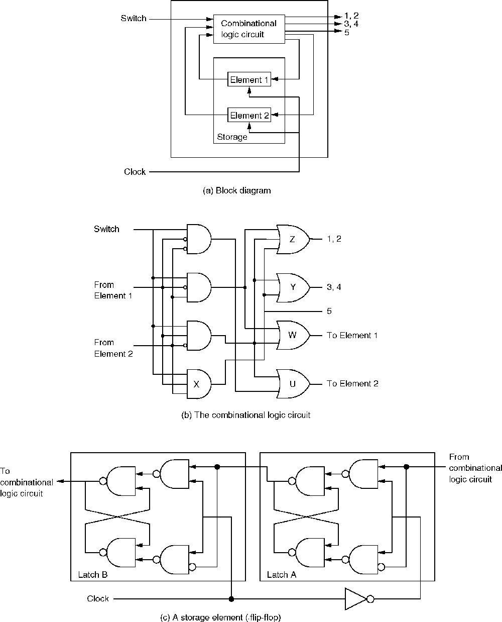
Muxes, decoders, and full adders are combinational logic circuits.
-
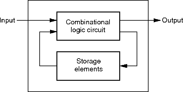
Combinational logic circuits have no capacity of storing information.
-
A different type, called sequential logic circuit, can, in addition to combinational logic, remember values and also base decisions on both input values and stored values.
-
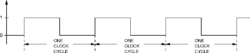
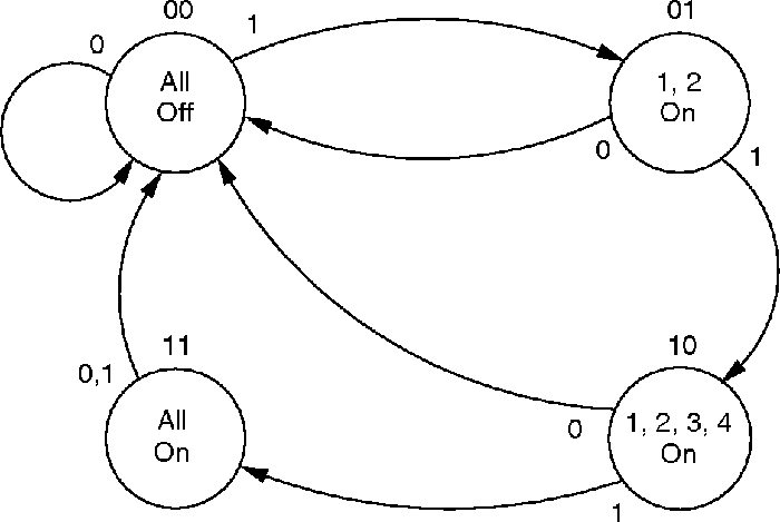
Sequential logic circuit: